- 您现在的位置:买卖IC网 > Sheet目录1991 > CS4362-KQZ (Cirrus Logic Inc)IC DAC 6CH 114DB 192KHZ 48LQFP
12
DS257F2
CS4362
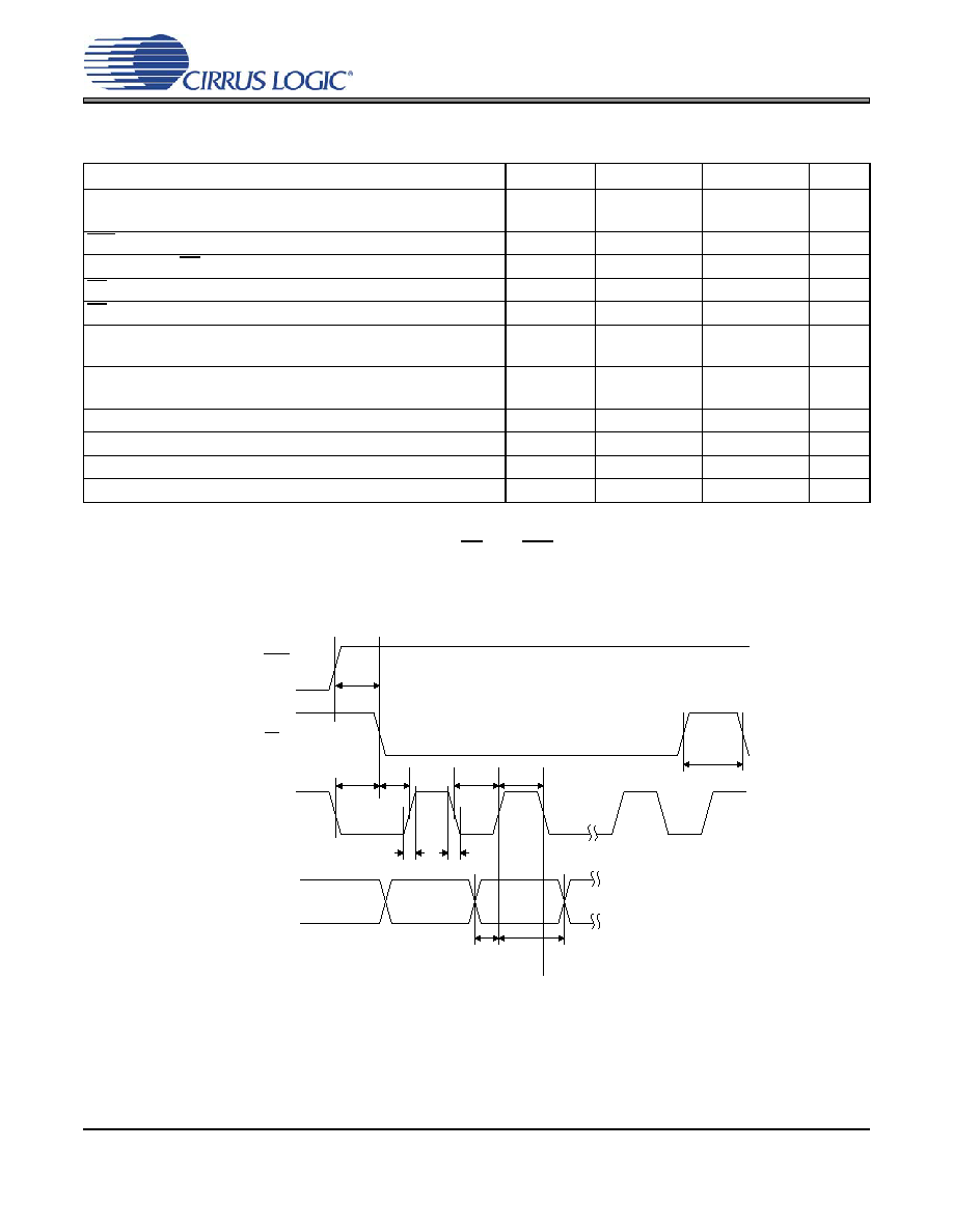
SWITCHING CHARACTERISTICS - CONTROL PORT - SPI FORMAT
(For KQZ TA = -10°C to +70°C; VLC = 1.8 V to 5.5 V; Inputs: Logic 0 = GND, Logic 1 = VLC, CL =30pF)
Notes:
22. tspi only needed before first falling edge of CS after RST rising edge. tspi = 0 at all other times.
23. Data must be held for sufficient time to bridge the transition time of CCLK.
24. For FSCK < 1 MHz.
Parameter
Symbol
Min
Max
Unit
CCLK Clock Frequency
fsclk
-
MHz
RST Rising Edge to CS Falling
tsrs
500
-
ns
CCLK Edge to CS Falling
tspi
500
-
ns
CS High Time Between Transmissions
tcsh
1.0
-
s
CS Falling to CCLK Edge
tcss
20
-
ns
CCLK Low Time
tscl
-ns
CCLK High Time
tsch
-ns
CDIN to CCLK Rising Setup Time
tdsu
40
-
ns
CCLK Rising to DATA Hold Time
tdh
15
-
ns
Rise Time of CCLK and CDIN
tr2
-
100
ns
Fall Time of CCLK and CDIN
tf2
-
100
ns
MCLK
2
-----------------
1
MCLK
-----------------
1
MCLK
-----------------
t r2
t f2
t dsu t dh
t sch
t scl
CS
CCLK
CDIN
t css
t csh
t spi
t srs
RST
Figure 4. Control Port Timing - SPI Format
发布紧急采购,3分钟左右您将得到回复。
相关PDF资料
CS4362A-DQZ
IC DAC 6CH 114DB 192KHZ 48-LQFP
CS4364-CQZR
IC DAC 103DB 24BIT 6CH 48-LQFP
CS4382A-DQZ
IC DAC 8CH 114DB 192KHZ 48-LQFP
CS4384-CQZR
IC DAC 8CH 103DB 192KHZ 48-LQFP
CS4385-DQZR
IC DAC 8CH 114DB 192KHZ 48-LQFP
CS4391A-KZZR
IC DAC 24BIT 192KHZ W/VC 20TSSOP
CS4392-KZZ
IC DAC 24BIT 192KHZ W/VC 20TSSOP
CS4397-KSZ
IC DAC 24BIT MULTY STNDRD 28SOIC
相关代理商/技术参数
CS4362-KQZR
功能描述:数模转换器- DAC IC 114dB 192kHz 6Ch DAC RoHS:否 制造商:Texas Instruments 转换器数量:1 DAC 输出端数量:1 转换速率:2 MSPs 分辨率:16 bit 接口类型:QSPI, SPI, Serial (3-Wire, Microwire) 稳定时间:1 us 最大工作温度:+ 85 C 安装风格:SMD/SMT 封装 / 箱体:SOIC-14 封装:Tube
CS4364
制造商:CIRRUS 制造商全称:Cirrus Logic 功能描述:103 dB, 192 kHz 6-Channel D/A Converter
CS4364_08
制造商:CIRRUS 制造商全称:Cirrus Logic 功能描述:103 dB, 192 kHz 6-Channel D/A Converter
CS4364-CQZ
功能描述:数模转换器- DAC IC 24bit 6Chn DAC w/ DSD Supt&Lw-Ltnc DF RoHS:否 制造商:Texas Instruments 转换器数量:1 DAC 输出端数量:1 转换速率:2 MSPs 分辨率:16 bit 接口类型:QSPI, SPI, Serial (3-Wire, Microwire) 稳定时间:1 us 最大工作温度:+ 85 C 安装风格:SMD/SMT 封装 / 箱体:SOIC-14 封装:Tube
CS4364-CQZR
功能描述:数模转换器- DAC IC 24b 6Ch DAC w/DSD Supt/Lw-Ltnc DF RoHS:否 制造商:Texas Instruments 转换器数量:1 DAC 输出端数量:1 转换速率:2 MSPs 分辨率:16 bit 接口类型:QSPI, SPI, Serial (3-Wire, Microwire) 稳定时间:1 us 最大工作温度:+ 85 C 安装风格:SMD/SMT 封装 / 箱体:SOIC-14 封装:Tube
CS4364-DQZ
制造商:CIRRUS 制造商全称:Cirrus Logic 功能描述:103 dB, 192 kHz 6-Channel D/A Converter
CS4364-DQZR
制造商:CIRRUS 制造商全称:Cirrus Logic 功能描述:103 dB, 192 kHz 6-Channel D/A Converter
CS4365
制造商:CIRRUS 制造商全称:Cirrus Logic 功能描述:114 dB, 192 kHz 6-Channel D/A Converter